
Task Requirements
You are an unfortunate student at Gourd University, and today is your first day of classes. As you walk into the classroom full of ambition, you glance at the unfamiliar circuit diagram on the big screen, not realizing what is about to happen.
But soon, you find out about the thunderbolt on a clear day! The teacher expects you, with no prior knowledge, to analyze the working principle of this power adapter based on the given schematic and relevant materials!
“Meow, meow, meow???” you exclaim anxiously, and the first thought that crosses your mind is to drop the course.
“Hmph!” the teacher sneers, “Don’t think I don’t know what you’re thinking! This is a required course, after all~”
Desperate, you collapse, realizing that the teacher even demands a physical report to be submitted on Wednesday, just two days from now! As you find yourself at a loss, you suddenly remember someone…
“No!” you scream in despair, “This can’t be!”
That someone is a famous cat foodie, and as the most attractive cat at Gourd University, you’ve been coveted by them for a long time. You know that if you go to them, you can solve your current difficulties… but at what cost?
Let’s Begin the Analysis
What is UC2842?
UC2842 belongs to the UCx84x series of integrated circuits, which is a famous design by TI (TEXAS INSTRUMENTS). It can be used in offline or DC-DC converter applications and is commonly used in switch-mode power supplies. It features a 30V, 1A, 500KHz current-mode PWM controller with support for 16/10V UVLO and 100% duty cycle. It can operate stably in the temperature range of -40 to 85 degrees Celsius.
In simple terms, UC2842 is a chip that can be used to design AC-DC/DC-DC converters.
According to the official website information, it comes in various packages and can operate with as few as 8 pins.

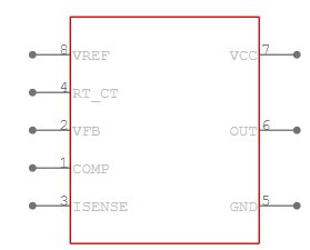
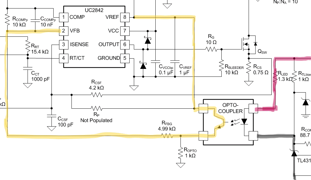
From the fourth image in the gallery above, we can see that this chip has different functions for its 8 pins, as follows:
| PIN | Pin Name | Function Description |
|---|---|---|
| 1 | COMP (Compensation) | Output pin responsible for external loop compensation |
| 2 | Voltage Feedback | Input signal applied to the inverting terminal of the error amplifier, provided by connecting a voltage divider to the power supply of the switching power supply. |
| 3 | SENSE (Current Sensing) | Connect this pin to the current sensing resistor, which is used to monitor the current in the circuit. The output voltage at the ends of the current sensing resistor provides the input signal to the PWM, which terminates the on-time of the output switch using this input signal. |
| 4 | RT/CT (Timing Resistor/Timing Capacitor) | This pin sets the switching frequency of the internal oscillator. Connect only a timing resistor, Rt, from pin 4 to ground and a timing capacitor, Ct, from pin 4 to ground. |
| 5 | GND | Ground |
| 6 | OUTPUT | It generates a PWM signal used to directly drive the gate of the power MOSFET. Totem pole configuration provides high current sink and source capability. |
| 7 | VCC | Connect to the positive supply pin. |
| 8 | VREF | Provides charging current to capacitor Ct through resistor RT. It has short-circuit protection and can provide 20mA (overcurrent) for powering additional control circuitry. |
How Does It Work?
Because we’re running out of time on the train and need to speed up, please refer to the TI document for detailed working principles and relevant formulas! Let’s move on to the analysis of the schematic diagram.
In fact, this document contains all the information about the chip, so you should definitely take a closer look at it.
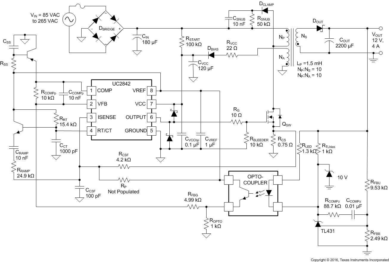
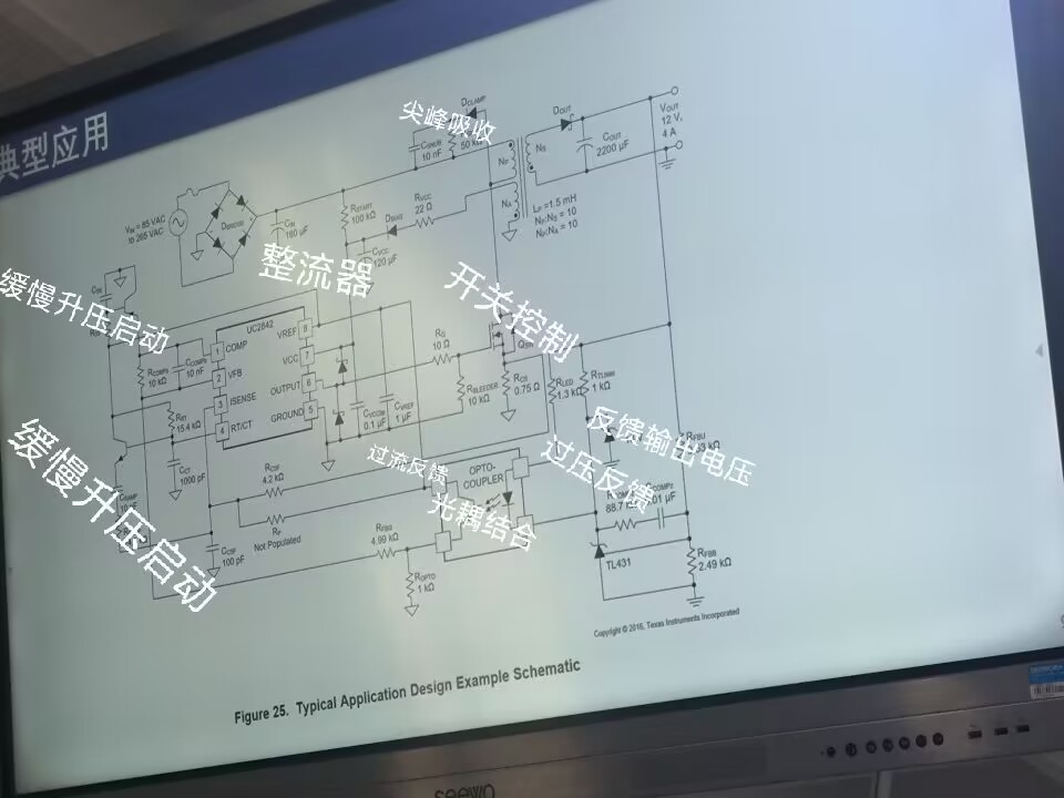
Analysis of Typical Applications
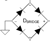
To make the chip work, we need to ensure it has the correct power supply. In a typical application, let’s assume an AC-DC scenario. The chip requires a direct current (DC) supply since its output is also DC. Therefore, we first need to convert AC to DC, which is achieved using a rectifier bridge.
To provide power, we also need to divide the obtained DC voltage. Here, a large resistor (100KΩ) is used for this purpose. If you’re interested, you can calculate the voltage range of the DC voltage obtained after this voltage division.
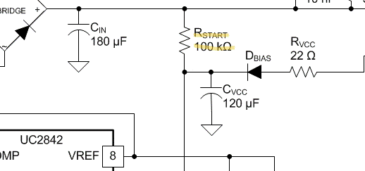
Since the AC input has a wide amplitude, the DC voltage obtained from voltage division may vary. To ensure that the voltage meets the chip’s requirements, we use a voltage regulator diode to make sure everything is stable.
Finally, we obtain a voltage at pin 7 of the chip that meets its operational requirements.
After obtaining the correct voltage at pin 7, pin 8, labeled as Vref, generates a 5V reference voltage.
From the diagram, you can see that this voltage passes through Rrt to pin 4 RT/CT, and simultaneously to Crt, with the other end of Crt connected to ground.
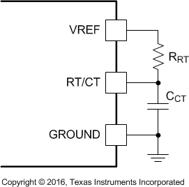
At the same time, pin 6 OUTPUT will output an oscillation wave based on the status of pin 4. This oscillation wave will switch the field-effect transistor.
Let’s shift our focus back to the 5V reference voltage generated at pin 8 Vref. Besides going to Rrt, it also goes to Rss resistor and Css capacitor. Their function is soft start, as indicated by SS, which stands for Soft Start.
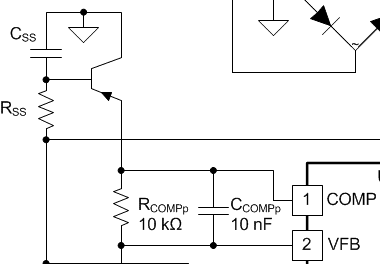
After passing through the Rss resistor, it charges the Css capacitor. Then, it slowly rises via a connected PNP transistor to pin 1 COMP, which is the positive feedback adjustment for the output voltage. It affects the output time of the OUTPUT pin. When the voltage feedback is higher, the OUTPUT pin remains on for a longer time, resulting in a higher output voltage.
Soft start ensures that the voltage at the output terminal rises slowly, preventing damage to connected devices due to sudden voltage surges.
Rramp and Cramp have similar functions.
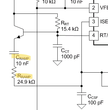
They ensure that the voltage at pin 3 ISENSE is above 1V when the chip is powered on. ISENSE is a current feedback pin, and when it’s above 1V, the OUTPUT is turned off.
This way, the 5V output from pin 8 has completed its task. As mentioned earlier, pin 6 OUTPUT outputs an oscillation wave. This wave drives the field-effect transistor, which, in turn, switches the coil, starting the operation of the transformer.
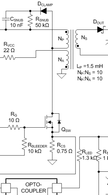
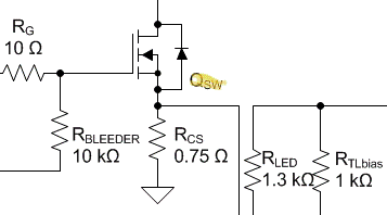
Under the combined action of Np and Na, a very high voltage is generated. To prevent this voltage from breaking down the field-effect transistor Qsw, we use Dclamp, Csnub, and Rsnub to form a snubber circuit.
Additionally, you may notice a small resistor Rcs below the field-effect transistor. Its purpose is for current sensing, typically using an alloy resistor with low temperature coefficient. The resistance value of the current sensing resistor is usually very small to avoid affecting the functional circuit.
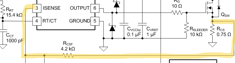
Depending on the current flowing through Rcs, a current sensing voltage is generated across its terminals. This voltage is then fed through Rcsf to pin 3 ISENSE. When the current becomes too high, the voltage at pin 3 exceeds 1V, which shuts off the output at pin 6, providing protection.
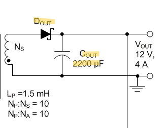
Next, let’s focus on the output section, which is relatively simpler. It includes a diode for reverse voltage protection, a capacitor for filtering, and ultimately provides power to the load.
You may also notice that an extra wire is led out from the output section, and it undergoes voltage division through two resistors.
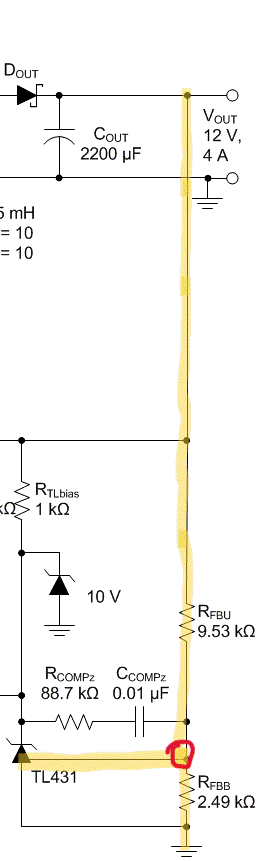
Based on calculations, when the output is 12V, the voltage at the red circle is approximately 2.48V. When the voltage exceeds 2.5V, the TL431 starts conducting. (TL431 and TL432 devices are three-terminal adjustable shunt regulators). Since the TL431 itself consumes some current, the upper Rtlbias provides the TL431 with the ability to cross the dead zone.
After TL431 conducts, the optocoupler device OPTO-COUPLER’s light-emitting diode (LED) turns on, affecting the phototransistor. This action allows the 5V VREF signal from pin 8, divided by resistors, to be fed back to pin 2 VFB. VFB is the negative feedback control pin for pin 6 OUTPUT. Lowering the voltage at VFB extends the time that pin 6 OUTPUT remains active. (The resistor Rp marked as “Not Populated” in the diagram is used for testing purposes and is not connected in actual applications).
Keen observers may notice that TL431 is also connected to a bypass.
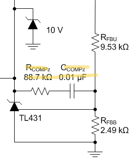
The purpose of this bypass is to improve the circuit’s dynamic response.
To sum it up visually:
Alright, I won’t keep you any longer. I’m off to eat some cat food now!!!