Purpose of writing
Introduction to SPINE
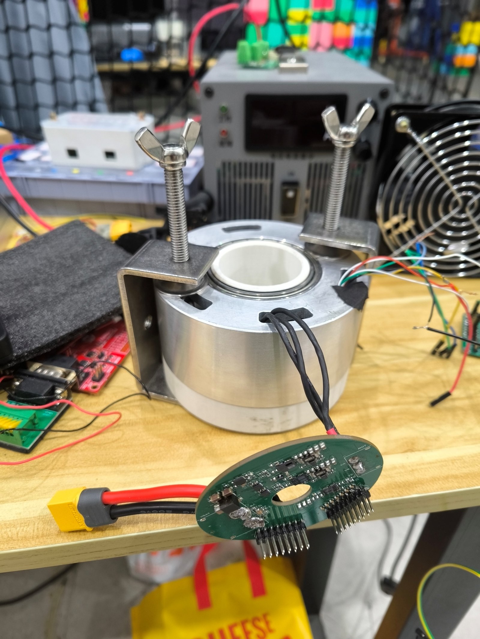
The MIT’s Cheetah quadruped robot is a project from the Massachusetts Institute of Technology’s Biomechatronics Lab, renowned for its outstanding speed, agility, and stability. A key component in its hardware architecture is the SPINE (Serial Peripheral Interface Network Extension) board, which acts as a protocol converter, transforming the SPI (Serial Peripheral Interface) communication protocol of the UPboard (a computing platform usually responsible for processing advanced control algorithms and decision-making logic) into the CAN (Controller Area Network) protocol required for motor control.
The SPI protocol is a common serial communication protocol used for communication between microcontrollers and various peripheral devices, such as sensors or other control modules. It conducts data exchange in a high-speed, synchronous, full-duplex manner, suitable for applications demanding high-speed data transmission.
The CAN protocol is a message-oriented protocol designed for communication between microcontrollers and devices, especially in complex systems like automobiles. It provides a highly reliable communication mechanism, capable of handling sophisticated error detection and conflict resolution mechanisms, ensuring the reliability and timeliness of data transmission in electronic systems.
In the hardware architecture of the Cheetah quadruped robot, the SPINE board serves to bridge these two different communication protocols, allowing the control algorithms based on the UPboard to send instructions via the SPI protocol. These instructions are then converted by the SPINE board and transmitted to the robot’s motors in the form of the CAN protocol.
Existing Problems
In 2016, MIT open-sourced their SPINE board hardware design. Dami Technology Co., Ltd., a domestic company, copied this open-source design with minor adjustments and produced their own version of the SPINE to sell. To reduce costs and facilitate production, they made the following changes to the original design:
- Changed the external high-speed crystal oscillator frequency from 12M to 8M.
- Replaced the STM32F446ZET6, which has more Flash size and GPIO numbers, with STM32F446RCT6.
- Removed the interface and chip that were default soldered for the remote control.
However, they did not make corresponding adjustments to MIT’s publicly released open-source code, leading to a series of issues after code modification. Moreover, they shipped the boards without pre-installed code for testing, resulting in disappointingly low product yields that depended heavily on luck.
To address the above issues, this guide provides instructions for reliable programming and testing of the SPINE 8M version.
Test Environment
| Item | Specification |
|---|---|
| Host Processor Architecture | AMD64/x86 |
| Host Software System | WINDOWS 7/8/10/11 |
| MCU Programmer Model | ST-LINK v2/v3 or J-Link/DAP (This guide does not provide instructions for these) |
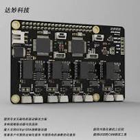
| SPINE Board Version | Dami SPINE 8M |
| Host Programming Software | STM32 ST-LINK Utility v4.6.0 |
Test Steps
1. Download STM32 ST-LINK Utility (STSW-LINK004)
The STM32 ST-LINK Utility (STSW-LINK004) provides an easy-to-use and efficient environment for reading, writing, and verifying storage devices, offering extensive functionality for programming STM32 internal memory (flash, RAM, OTP, etc.), external memory, verifying programming content (checksum, during and post-programming verification, comparison with file), and automating STM32 programming.
We need this software to read and program the modified FLASH area of the chip.
For convenience, a copy of the software is mirrored in a storage bucket. Please do not distribute this link as it has a monthly traffic limit of 100G. Alternatively, you can click on the download link at the beginning of the article to download all the necessary files.
2. Install STM32 ST-LINK Utility (STSW-LINK004)
After downloading, you will get setup.exe (from the official link) or STM32 ST-LINK Utility v4.6.0.exe (from the mirror link). Double-click to start the installation.
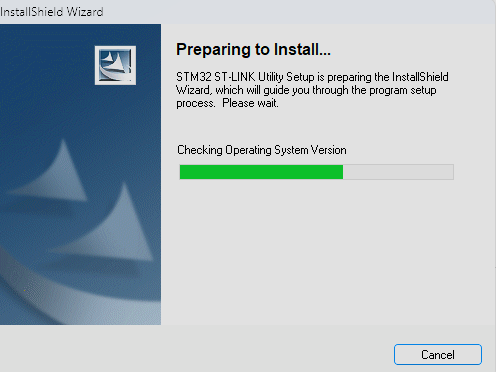
Figure 1 Installation of ST-LINK Utility
3. Download the Stable SPINE 8M Firmware
To ensure that the code downloaded into the chip is correct and unaffected by the compiler or code versions, a binary file has been compiled. This binary file’s code version has been thoroughly tested, and the compilation environment is stable and controlled. Programming this binary file into the hardware ensures that we can correctly and reliably test the SPINE 8M hardware.
After downloading, you will receive the Spine8M.bin file. Alternatively, you can click the download link at the beginning of the article to download all necessary files.
4. Establish Connection and Program the Chip Using ST-LINK
Open the ST-LINK Utility software and enter the main interface.
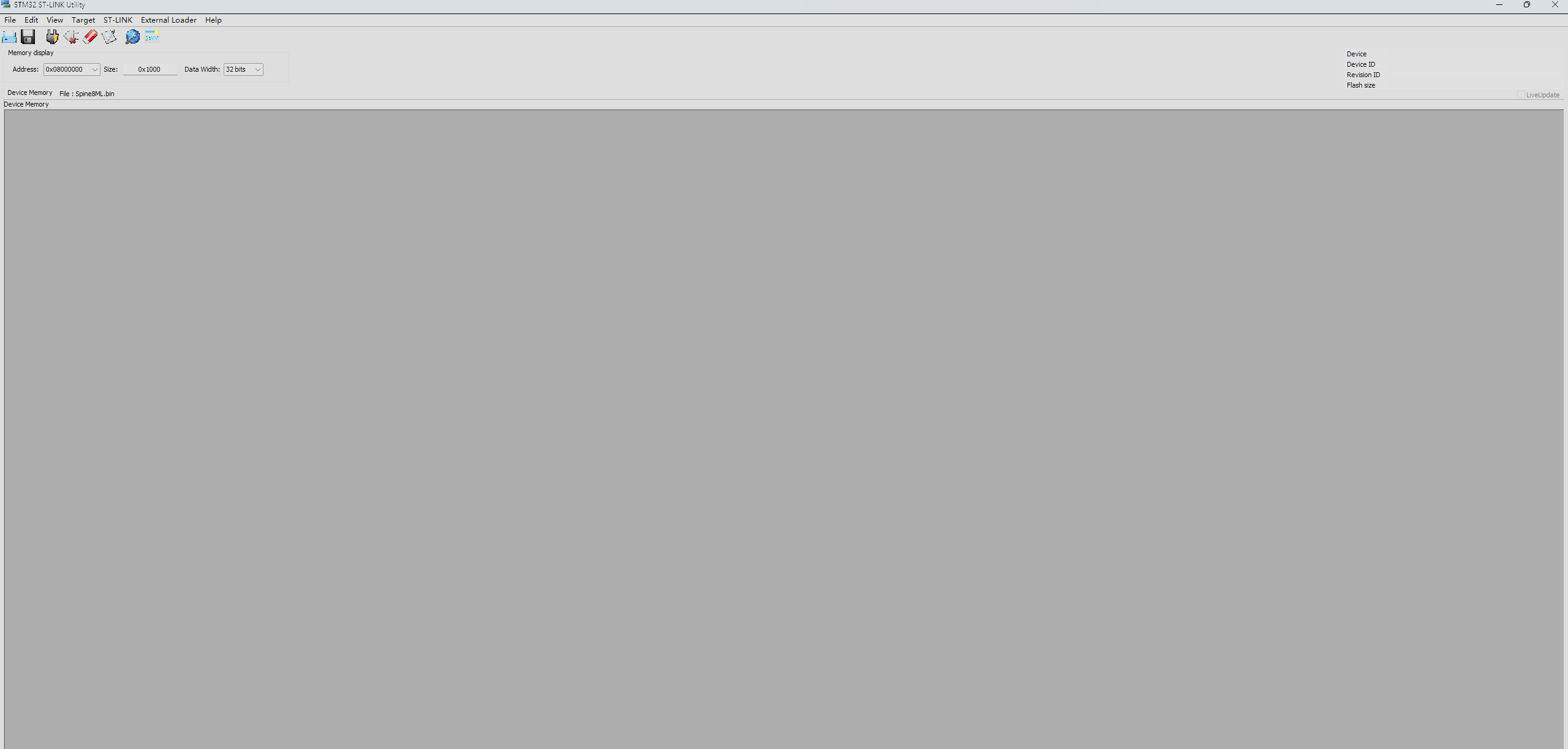
Figure 2 ST-LINK Utility Main Interface
Consulting the manual, we know that the STM32F446RCT6 has a FLASH capacity of 256kb. Therefore, we should change the size in the top-left corner from 0x1000 to 0x40000.
All STM32 have a 32-bit width, and the user FLASH starting address is always 0x08000000, so these do not need to be changed.
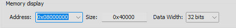
Figure 3 ST-LINK Utility Address, Size, and Width Settings
After modifying the parameters as shown above, insert the ST-LINK into the STM32’s SWD programming and debugging port. Click “Connect to the target”.
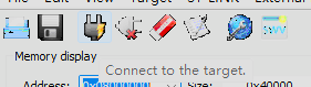
Figure 4 ST-LINK Utility Connecting to the Chip
If an error “No ST-LINK detected” appears, please replug the ST-LINK or check if it is damaged.
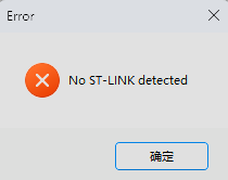
Figure 5 ST-LINK Utility Connection Error 1
If an error “Can not connect to target!” appears, please check the connection between the ST-LINK and the STM32 SWD.
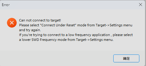
Figure 6 ST-LINK Utility Connection Error 2
If everything is normal, the corresponding STM32 chip’s FLASH data should be read and displayed.
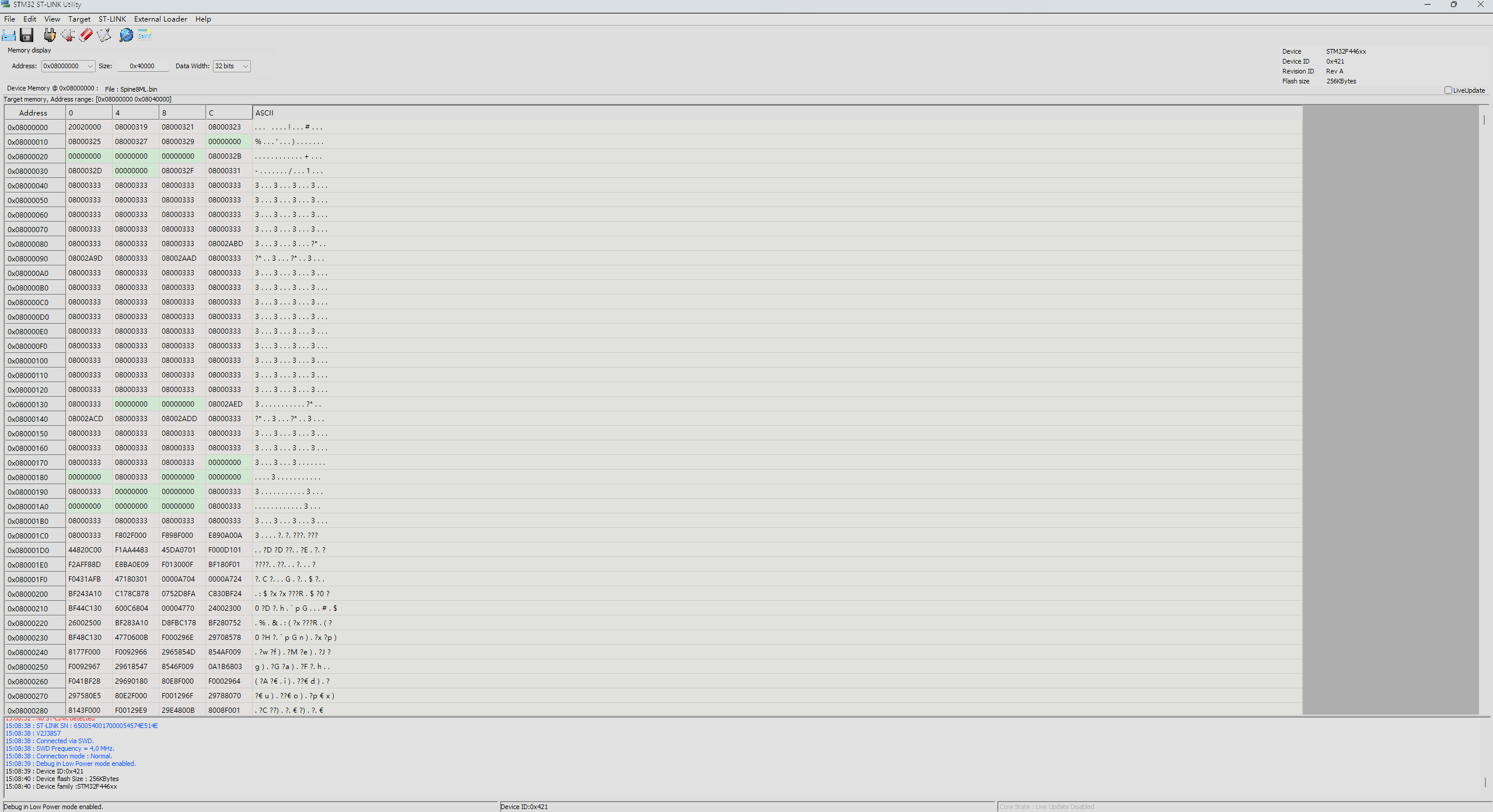
Figure 7 ST-LINK Utility Successful Connection
Next, select Target > Program & Verify…
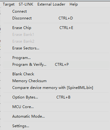
Figure 8 Select Target > Program & Verify…
Select the recently downloaded Spine8M.bin, confirm other settings are correct, and then click Start to begin programming.
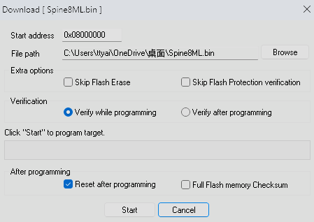
Figure 9 Programming the Firmware into the Chip
After the download completes, wait a few seconds and disconnect if there are no error messages. Following the fourth step, program the second chip, then connect to the Upboard and follow the content in the Arcdog Software repository to test the SPINE.